a) Left: representative SEM image of silica opal on a patterned Si
5 (534) · € 33.50 · Auf Lager

Download scientific diagram | (a) Left: representative SEM image of silica opal on a patterned Si substrate with complex geometry. Right: Fourier transform of a marked region (about 17 spheres × 17 spheres) in an SEM image. (b) Left: SEM image of the same silica opal on another area of the patterned Si substrate. Right: Fourier transform of a marked region (about 38 × 10 spheres) in an SEM image. (c, d) Fourier transform of Figure 1a. (c) Large marked region (about 70 μ m × 50 μ m). (d) Small marked region (about 10 spheres × 10 spheres). from publication: Integration of Self-Assembled Three-Dimensional Photonic Crystals onto Structured Silicon Wafers | We report on the fabrication of high-quality opaline photonic crystals from large silica spheres (diameter of 890 nm), self-assembled in hydrophilic trenches of silicon wafers by using a novel technique coined a combination of "lifting and stirring". The achievements reported | Silicon Wafer, Photonic Crystals and Self-Assembly | ResearchGate, the professional network for scientists.

IJMS, Free Full-Text

Colloidal Self-Assembly of Highly-Ordered Silica Inverse Opals for Deep Ultraviolet Diffraction

IJMS, Free Full-Text

Full article: 2D and 3D photonic crystal materials for photocatalysis and electrochemical energy storage and conversion
Minerals, Free Full-Text

Preparation of Monodisperse Silica Nanoparticles via Controlling the Interphase of Two-Phase Synthesis for Optical Anticounterfeiting Materials

Colloidal Crystal Films: Advances in Universality and Perfection

Revealing salt-expedited reduction mechanism for hollow silicon microsphere formation in bi-functional halide melts
Materials, Free Full-Text

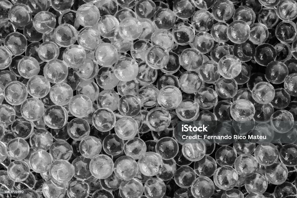
SEM image of initial opal matrix formed by silica spheres with diameter